


Designing digital electronics, embedded systems, or real-time software protocols requires precise control over time. A Timing Diagram visualizes how digital signals or software states change over a specific timeline, making complex hardware interactions and signal conditions clear.
By leveraging an AI Chatbot, you no longer need to manually align signal pulses, draw transition lines, or calculate clock cycles. You can convert plain-text signal specifications, communication protocols, or timing requirements into fully structured Timing Diagrams in seconds using simple conversational prompts.
What is a Timing Diagram?
A Timing Diagram is a behavioral diagram that tracks the state of signals or components along a horizontal time axis. It clearly illustrates exact time constraints, clock cycles, propagation delays, and state changes between interconnected hardware components or software processes.
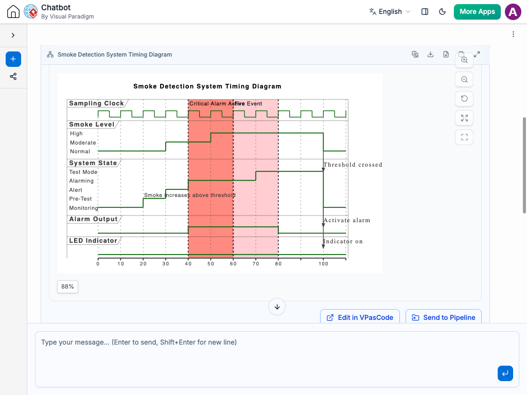
Key Components of a Timing Diagram
-
Time Axis: The horizontal axis representing elapsed time, divided into clock cycles or specific time units.
-
Signals / Lifelines: Horizontal tracks representing digital inputs, outputs, clock lines, or software states.
-
High/Low Logic States: Visual waveform transitions showing binary logic high (1), logic low (0), or bus values.
-
Clock Signals: Continuous oscillating square waves used to synchronize state transitions.
-
Timing Constraints: Annotations indicating setup times, hold times, propagation delays, or pulse widths.
Why Use Timing Diagrams?
Visualizing system state changes across exact time intervals provides critical advantages during system design and debugging:
-
Eliminate Signal Race Conditions: Identifies timing overlaps, setup violations, and hold-time conflicts before building hardware.
-
Simplify Complex Protocols: Provides a visual reference for hardware communication standards like SPI, I2C, UART, and bus transfers.
-
Streamline Hardware & Firmware Handoffs: Gives digital logic engineers and firmware developers a shared understanding of hardware timing requirements.
-
Accelerate Embedded Debugging: Helps teams diagnose intermittent timing bugs by comparing expected signal waveforms against live oscilloscope readings.
Common Real-World Use Cases
Timing Diagrams are widely used across embedded engineering, hardware design, and low-level software development:
-
Microcontroller Bus Interfaces: Mapping memory read/write cycles, address buses, and data bus latching.
-
Communication Protocols: Visualizing data transmission frames, start/stop bits, and clock edges for SPI, I2C, or CAN protocols.
-
Digital Logic Design: Modeling flip-flops, registers, counters, and state machine transitions.
-
Real-Time Software Threads: Tracking task execution, interrupt requests (IRQ), and thread scheduling in RTOS applications.
How to Generate Timing Diagrams Using AI Chatbot
Creating a Timing Diagram with Visual Paradigm’s AI Chatbot takes just a few simple steps:
-
Open the AI Chatbot Workspace: Launch the diagramming workspace in your browser.
-
Describe Your Timing Specification: Enter your signal behavior, clock cycles, or protocol sequence directly into the AI Chatbot window.
-
Specify the Diagram Type: Tell the AI Chatbot to generate a “Timing Diagram.”
-
Review and Render: The AI Chatbot parses your specifications and builds the timing waveform automatically.
-
Refine with Natural Language: Ask the AI Chatbot to adjust clock frequencies, add delays, or rename signal tracks using quick chat commands.
Practical AI Chatbot Prompt Examples
Try using these prompt statements inside the AI Chatbot to generate instant Timing Diagrams:
Example 1: SPI Data Read Transfer Cycle
Create a Timing Diagram for an SPI data read transfer, covering a Clock signal oscillating across 8 cycles, a Chip Select signal driving Low to start the frame, a Master Out Slave In signal sending an 8-bit read command on rising clock edges, and a Master In Slave Out signal returning data bits on falling clock edges.
Example 2: Memory Write Access Cycle
Create a Timing Diagram for a memory write access cycle, showing an Address Bus setting the memory address at T1, a Write Enable signal pulsing Low at T2, a Data Bus placing data at T2, and all signals resetting to idle at T4 after a 2-cycle hold time.
Best Practices for Designing Clear Timing Diagrams
To keep your timing diagrams clear, precise, and easy to analyze, follow these guidelines:
-
Align Transitions with Clock Edges: Ensure state changes clearly reference whether they trigger on rising, falling, or level clock signals.
-
Group Related Signals: Stack related signal lines together (e.g., placing clock, chip select, and data signals adjacent to each other).
-
Label Timing Constraints Explicitly: Include clear markers for critical parameters like setup time ($t_{su}$), hold time ($t_h$), and propagation delay.
-
Keep Bus Representations Clean: Use crossed lines or shaded blocks to represent multi-bit data buses rather than drawing individual signal traces.